In the heart of every digital device lies a silent yet powerful enabler: the Printed Circuit Board (PCB). It is the skeleton of modern electronics—whether in your smartphone, your laptop, a medical device, or even satellites. But few outside the tech world truly understand the complexity and precision behind printed circuit board fabrication.
Fabricating a PCB isn’t just printing lines on a fiberglass sheet; it’s a multi-step engineering feat that fuses physics, chemistry, electronics, and automation into a harmonized process. Each trace, each drilled hole, each protective mask has a purpose. When done right, it results in boards that can last for years without failure—even under extreme conditions.
The Role of PCBs in Modern Electronics
PCBs provide the electrical backbone for virtually every electronic circuit. They:
-
Physically support components like resistors, capacitors, and ICs.
-
Electrically connect them using copper traces and vias.
-
Enable miniaturization, consistency, and mass production of devices.
In the IoT age, PCBs must be compact, high-performing, and able to handle both analog and digital signals, sometimes on the same board. From wearable tech to industrial machines, reliable PCB fabrication ensures these devices perform without hiccups.
Types of Printed Circuit Boards
Depending on application, PCBs vary in complexity and composition:
-
Single-layer PCBs: Basic, cost-effective, great for calculators or LED circuits.
-
Double-layer PCBs: More density, suitable for control systems or audio equipment.
-
Multilayer PCBs: Up to 30+ layers, for servers, aerospace, and complex electronics.
-
Rigid PCBs: Standard boards with solid base materials.
-
Flexible PCBs: Bendable, used in foldable phones, medical devices.
-
HDI Boards: High-density interconnect boards with microvias and fine lines for high-speed applications.
Design Stage: Blueprinting the Circuit
Before manufacturing begins, engineers create a schematic diagram representing the electronic circuit. They convert this into a layout using EDA software, positioning components and routing electrical traces between them.
Important here is DFM (Design for Manufacturing). Design must consider trace width, spacing, drill sizes, layer stack-up, and thermal behavior to avoid future fabrication errors.
Software Tools Used in PCB Design
PCB design heavily depends on reliable software. Popular options include:
-
Altium Designer: Industry standard with powerful 3D visualization.
-
KiCad: Open-source tool popular among hobbyists and startups.
-
Eagle (by Autodesk): Great for small businesses and makers.
-
OrCAD: Strong signal integrity analysis tools.
These platforms help generate Gerber files, which are essentially the machine language for fabricators.
Gerber Files: The Language of Fabrication
Gerber files contain instructions for each PCB layer: copper paths, solder mask, drill holes, silkscreen, and more. Each file corresponds to one manufacturing operation. Missing or incorrect Gerbers can derail the entire fabrication process, making proper file preparation crucial.
Material Selection for PCB Fabrication
A PCB is more than copper and fiberglass. Common materials include:
-
FR4: The most popular substrate, flame-retardant and durable.
-
Polyimide: Used in flexible PCBs for high-heat environments.
-
Copper Foil: The conductive layer etched into traces.
-
Solder Mask: Protective layer that insulates copper paths.
-
Silkscreen Ink: Adds visual identifiers and orientation marks.
Material selection affects everything from signal quality to thermal resistance.
Substrate Preparation and Copper Cladding
The fabrication begins by cleaning the substrate to remove dust and oxidation. Then, a thin sheet of copper is laminated onto one or both sides using high pressure and heat. This copper layer forms the base for creating electrical traces.
Photoresist Application and UV Exposure
A light-sensitive film called photoresist is applied to the copper. When exposed to UV light through the circuit pattern film, the photoresist hardens in the shape of the desired traces. The unhardened areas are then washed away, exposing the copper underneath.
Developing and Etching
Once patterned, the board is exposed to an etchant solution (usually ammonium persulfate or ferric chloride) that removes unwanted copper, leaving only the traces protected by hardened photoresist. This defines the circuitry on the layer.
Layer Alignment and Lamination
For multilayer PCBs, this step is critical. Inner layers are aligned using optical registration systems and laminated together with prepreg (a bonding resin layer). The stack is pressed under heat and pressure in a vacuum to avoid air gaps.
Drilling Holes and Vias
Precision CNC drills or laser drills make holes for component leads and vias. Microvias connect high-density inner layers, while through-holes connect all layers. Tolerances are tight—fractions of a millimeter—so accuracy is everything.
Desmearing and Electroless Copper Plating
Drilling leaves behind epoxy debris called smear, which must be removed to ensure good electrical contact. Once clean, the entire board (including holes) is coated with a thin layer of copper via a chemical process called electroless plating.
Plated Through-Hole and Electroplating
Now, electroplating thickens the copper in holes and on surface layers to the desired level. This strengthens traces and ensures reliable inter-layer connections, especially in complex multilayer boards.
Outer Layer Imaging and Etching
Just like the inner layers, the outer layers are patterned with photoresist and exposed to UV light to define traces. However, these layers include the final pads and copper connections to which components will be soldered. After exposure and development, copper is plated again, followed by etching to remove the excess copper and define the final circuit paths.
Solder Mask Application
Now that the circuitry is defined, a solder mask—usually green—is applied over the board to insulate copper traces and prevent solder bridges during component assembly. It’s applied as a liquid and hardened under UV light, exposing only the pads and vias needed for soldering.
Silkscreen Printing
Silkscreen adds the final layer of visual information to the PCB. It includes component labels, pin identifiers, logos, and any text that helps during assembly and maintenance. This is usually printed in white ink, though other colors are available.
Surface Finishes for PCBs
To protect exposed copper and ensure solderability, the PCB undergoes surface finishing. Common options include:
-
HASL (Hot Air Solder Leveling): Coats exposed copper with solder.
-
ENIG (Electroless Nickel Immersion Gold): Offers flat finish and long shelf life.
-
OSP (Organic Solderability Preservatives): A cost-effective, eco-friendly finish.
Each has pros and cons, depending on application, cost, and production volume.
Electrical Testing for Quality Control
Before delivery, PCBs must pass electrical tests to ensure there are no shorts or open circuits. This is typically done using:
-
Flying Probe Testers: For prototypes or low-volume runs.
-
Bed-of-Nails Testers: For high-volume production using a fixed fixture.
Every trace is verified against the original netlist to confirm electrical integrity.
Final Inspection and AOI
Visual inspection alone isn’t enough. That’s why fabricators use Automated Optical Inspection (AOI) systems to scan the board for defects like:
-
Misaligned traces
-
Excess solder
-
Broken pads
-
Unconnected vias
Manual inspection is done last, ensuring human oversight before packaging.
Panelization and Routing
To optimize manufacturing, multiple boards are often produced on one panel. After fabrication, these are separated using:
-
V-scoring: Creates a groove for easy breaking.
-
CNC routing: Cuts each board out precisely.
This step ensures uniformity and protection during shipping and assembly.
Cleaning, Packaging, and Shipping
Post-processing involves a final cleaning using deionized water or solvents to remove flux, dust, and particles. Boards are then vacuum-sealed, packed with ESD protection, and labeled for delivery. Some manufacturers also provide traceability data, including fabrication logs and inspection reports.
Environmental Standards and Compliance
Modern PCB manufacturers must comply with international regulations:
-
RoHS (Restriction of Hazardous Substances)
-
REACH (Registration, Evaluation, Authorisation, and Restriction of Chemicals)
-
ISO 9001/14001 for quality and environmental management
Proper waste disposal, chemical recycling, and worker safety procedures are integral to responsible fabrication.
Future of PCB Fabrication
The industry is evolving fast. Expect to see:
-
Flexible hybrid electronics: Combine rigid and bendable zones.
-
Embedded components: Smaller boards with integrated parts.
-
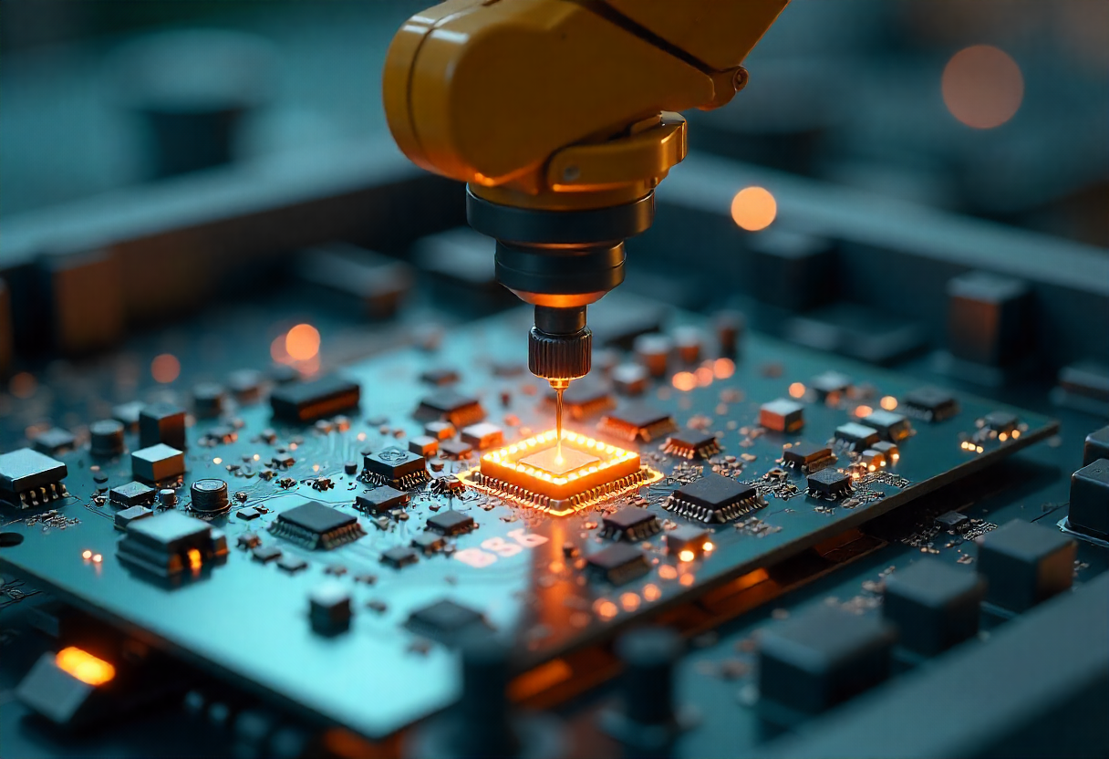
AI-powered fabrication: Improve yield and defect detection.
-
Green PCBs: Recyclable, biodegradable materials.
As devices shrink and grow smarter, PCB fabrication will only grow more advanced, pushing boundaries of engineering and sustainability.
Conclusion
The printed circuit board fabrication process is more than just copper and fiberglass—it’s an intricate dance of design, chemistry, precision, and innovation. From software to solder masks, from substrate to silkscreen, every step requires attention to detail and engineering discipline.
Understanding the full scope of PCB fabrication is not just beneficial—it’s essential for anyone working in or around electronics. Whether you’re a designer, engineer, or simply curious, you now know what goes into building the circuit boards that power the modern world.
FAQs
What is PCB fabrication?
PCB fabrication refers to the process of manufacturing the bare circuit board before electronic components are added.
How long does PCB fabrication take?
Typical turnaround is 3–7 days for standard boards, though express services can deliver in 24–48 hours.
What is the difference between PCB fabrication and assembly?
Fabrication builds the raw board; assembly adds and solders components onto it.
Which surface finish is best for PCBs?
ENIG is preferred for its flatness and durability, while HASL is more economical for general use.
What is the most common PCB material?
FR4 (a fiberglass-reinforced epoxy laminate) is the industry standard for most boards.
Can PCBs be recycled?
Partially. Copper and metals can be extracted, though traditional boards are difficult to recycle fully. New green PCB technologies aim to change that.